









Laser 3D Vision Empowers Semiconductor Intelligent Manufacturing
PCB & Semiconductor
Aug 21,2026
——Raychao High‑Tech Line‑Laser 3D Inspection Solution for Die‑Attach Quality Control
As the semiconductor industry advances toward high density and high reliability, increasingly stringent requirements are imposed on placement accuracy and quality control within chip packaging and manufacturing.
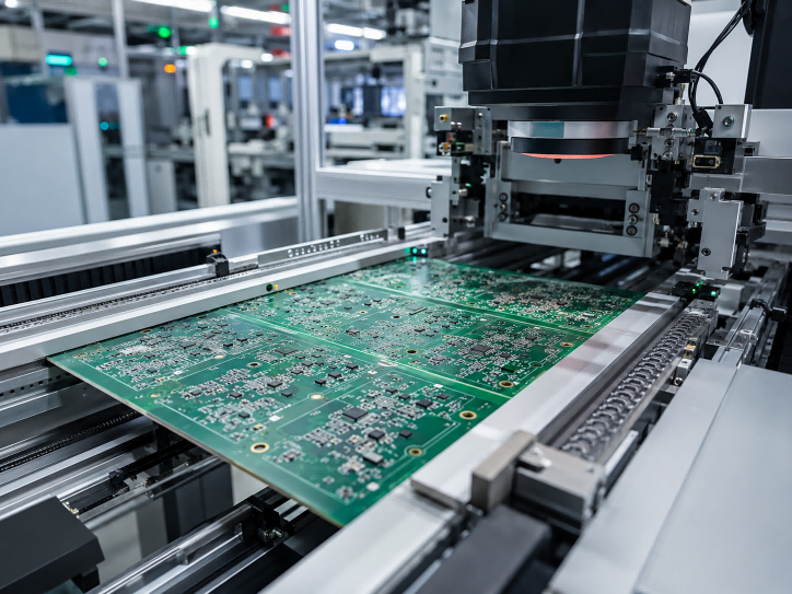
In production processes such as chip placement and die bonding, anomalies including chip position offset, chip warpage, stacked chips and missing chips directly impair subsequent bonding, electrical performance testing and overall product reliability. Accordingly, high‑speed, high‑precision, stable and reliable in‑line inspection has become a critical requirement for semiconductor intelligent manufacturing.
I. From 2D Vision to 3D Inspection: Breaking the Limitations of Conventional Inspection
Traditional 2D vision inspection performs judgements mainly based on image grayscale, edge and texture information, and exhibits inherent limitations for defects involving height variation, warpage and stacked chips.
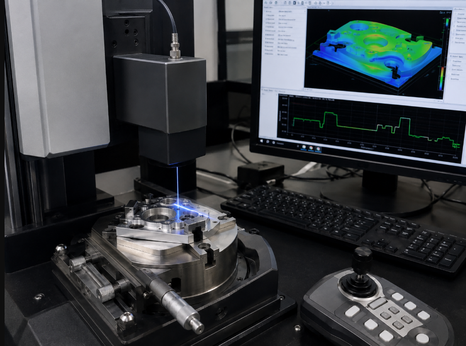
3D laser profile inspection acquires height information of object surfaces and elevates inspection from 2D images into 3D space, enabling:
Chip position offset detection
Chip angular deflection detection
Chip warpage detection
Stacked‑chip detection
Missing‑chip detection
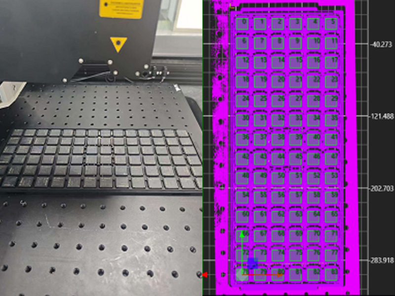
With 3D point clouds of chip surfaces obtained via laser scanning, the system analyses height variations directly to realise reliable identification of complex defects.
II. High‑Speed Line‑Laser Sensor for Micron‑Level 3D Measurement
This solution adopts the high‑precision line‑laser profile sensor LS2215.
Key Specifications:
‑ X‑axis resolution: 73 μm
‑ Working distance: 114 mm
‑ Laser line width: 126 mm ~ 174 mm
‑ Maximum scan frequency: 8 kHz
Following high‑speed laser scanning, the system generates 3D point clouds of chip surfaces and performs algorithm‑driven analysis of height differences to deliver high‑speed in‑line inspection.
Compared with conventional vision solutions, 3D laser inspection offers the following advantages:
Independence from surface texture
Judgement is based on height information regardless of variations in chip colour or reflectivity.
Direct 3D dimensional measurement
Height‑related anomalies such as warpage and stacked chips can be quantified directly.
Strong immunity to workpiece deformation
Fitting of the reference plane effectively mitigates inspection interference caused by minor substrate deformation.
III. Intelligent Algorithms for Stable Inspection under Complex Operating Conditions
Automatic chip position compensation
By identifying chip edge features, the system calculates X‑axis offset, Y‑axis offset and chip rotation angle, achieving automatic inspection‑region matching and improving inspection stability.
Reference‑plane fitting to eliminate substrate‑deformation effects
PCBs or carriers may experience slight bending during actual production. The system builds a reference plane using height data sampled from multiple regions and converts absolute chip height into relative height differences for enhanced inspection reliability.
IV. Multi‑Category Chip Inspection Covering Diverse Size Requirements
For chips of different sizes, the system configures multiple inspection zones and identifies anomalies through height and step‑height analysis.
Supported applications:
‑ Large‑size chip inspection
‑ Medium‑small‑size chip inspection
‑ Micro‑chip inspection
Even for micro‑chips at the 2 mm scale, height‑based analysis can reliably distinguish normal, missing, stacked and warped states.
V. Advancing Intelligent Inspection for Semiconductor Manufacturing
Semiconductor manufacturing is evolving toward higher precision, faster throughput and superior reliability.
Drawing on years‑long expertise in industrial 3D vision, Raychao High‑Tech delivers for the semiconductor industry:
‑ High‑precision laser 3D measurement technology
‑ High‑speed in‑line inspection solutions
‑ Customised vision algorithms
‑ Multi‑size chip compatibility
‑ Robust data‑analysis systems
Ranging from chip placement to packaging inspection, and from position compensation to defect identification, 3D laser vision has become a vital technical enabler for semiconductor intelligent manufacturing.
Raychao High‑Tech
Make industrial inspection more accurate. Make intelligent manufacturing more reliable.