

Everything you need to know about Litronics products.
Custom laser sources, optical engines and 3D measurement solutions for industrial imaging, projection and precision inspection.
OverviewEverything you need to know about Litronics products.
Overview
Our manuals detail product functions and settings for best performance.

Our manuals detail product functions and settings for best performance.

Our manuals detail product functions and settings for best performance.

Our FAQ section provides product information for users at all experience levels.
Get more news about Litronics and related industries.
Overview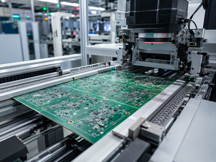
Measurement tasks in the semiconductor industry require highest accuracy and repeatability. Micro-Epsilon offers the right solution……
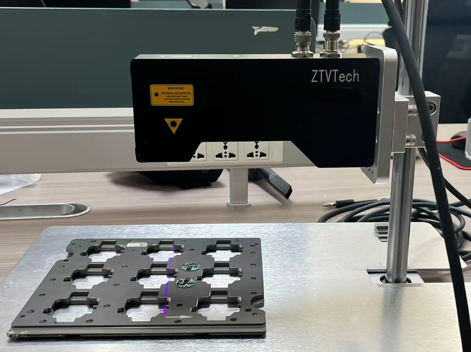
Perform online inspection of the height of soldered components at three locations on a PCB; the system must be capable o...
Learn More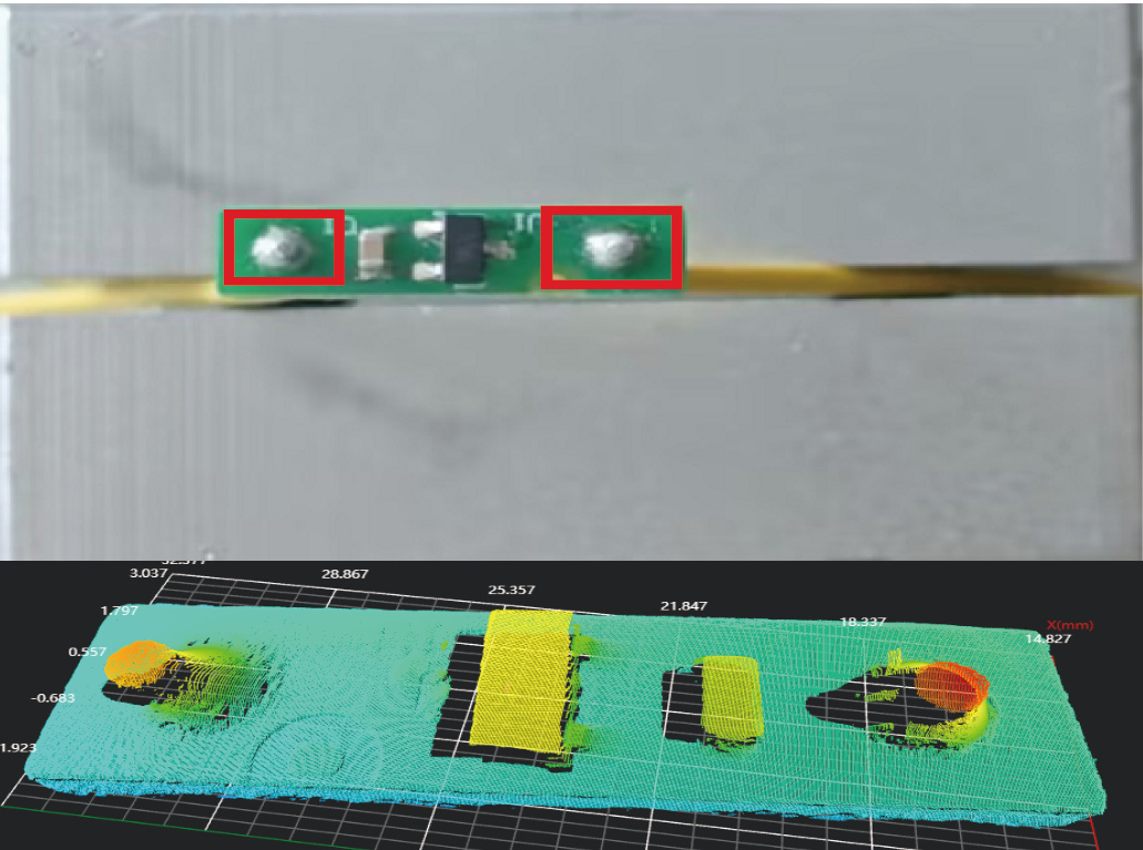
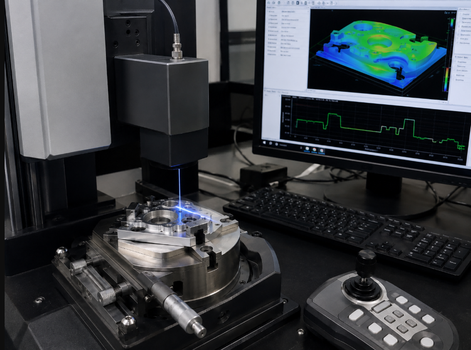
3D height inspection for PCB surface features including solder joints, assembled components and copper traces. It verifi...
Learn More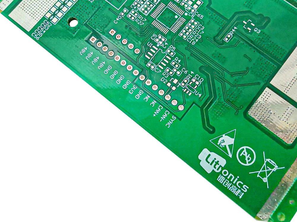
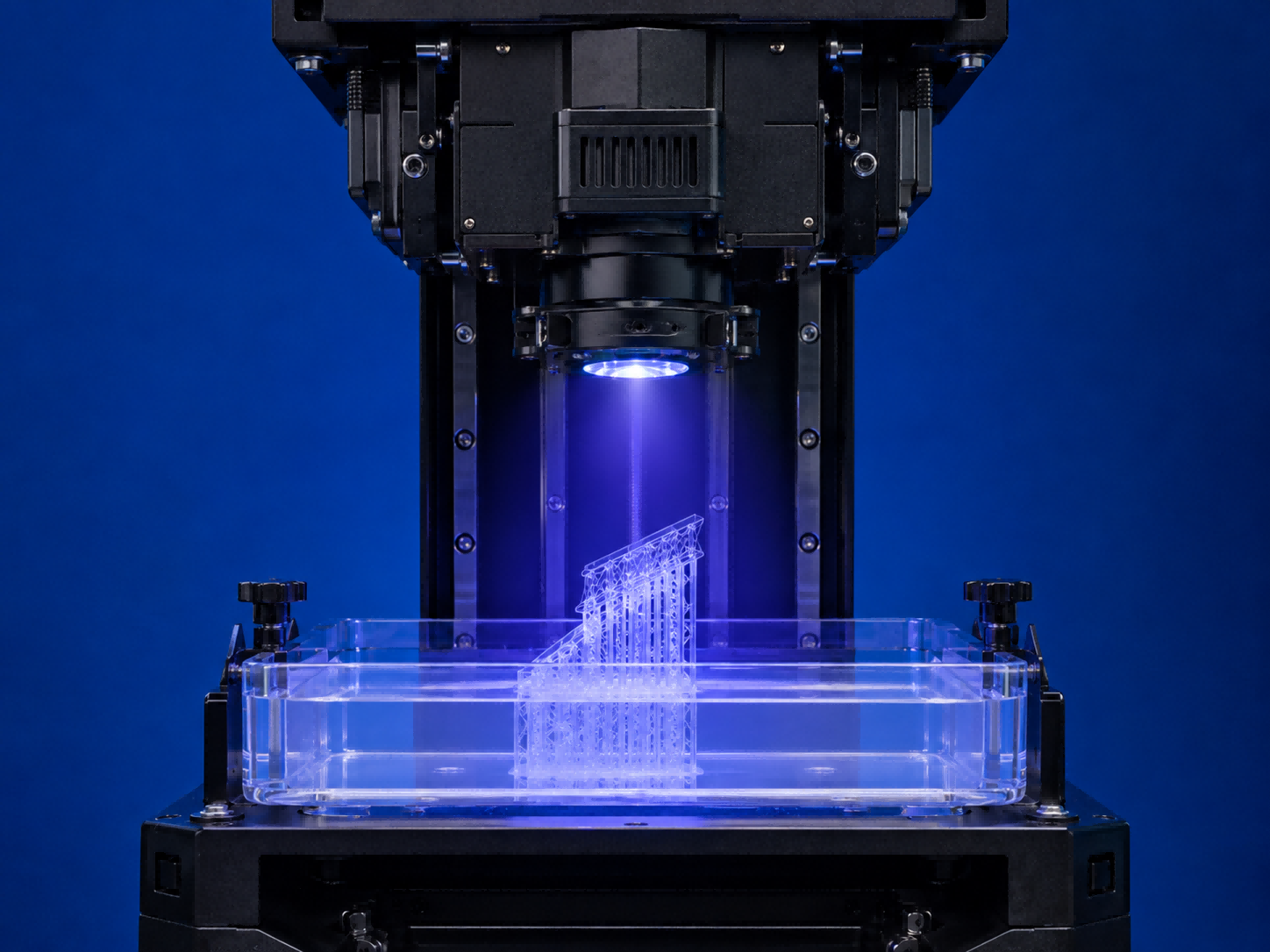
Mask‑free laser exposure technology. It directly generates high‑resolution patterns on PCB and various special substrate...
Learn More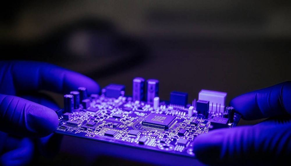
Specialized lithography solution for MEMS device manufacturing. It achieves high‑precision patterning of micro‑scale str...
Learn More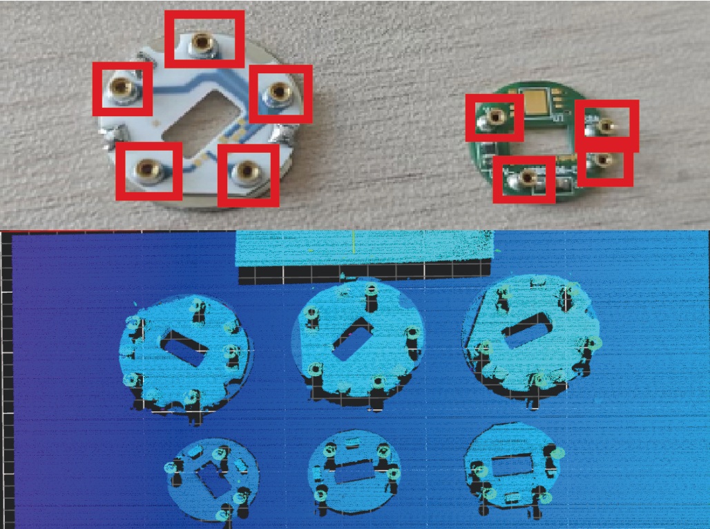
High‑precision 3D measurement of connector and component pins. It inspects pin height deviation, tilt and offset to guar...
Learn More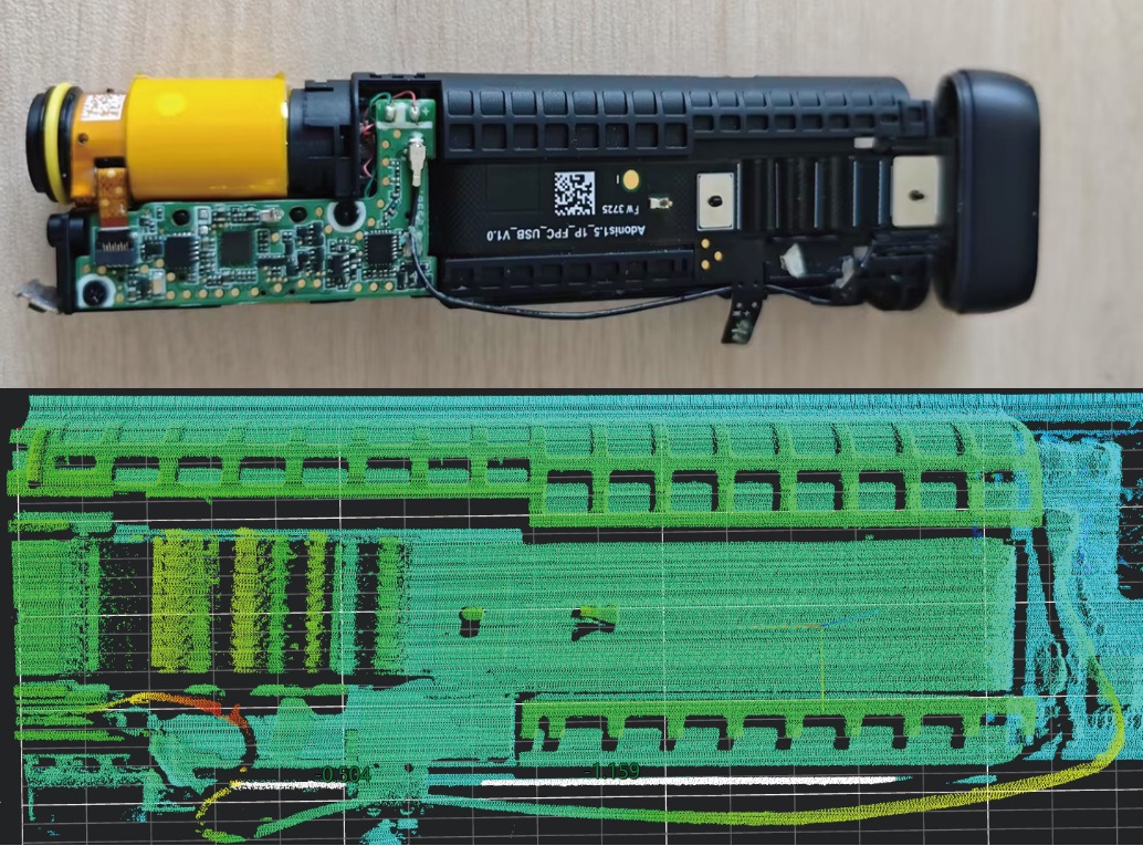
3D visual inspection for semiconductor bonding wires. It identifies wire sag, deformation, breakage and abnormal morphol...
Learn More
As an OEM partner, we can also develop and produce customized laser imaging, 3D measurement and optical module solutions according to your needs.
Contact Our Experts