












Application Specification Document for LDI Exposure Machines in PCB Solder‑Mask Manufacturing
Product Details
Aug 21,2026
1. Technical Overview and Industry Background
1.1 Core Functions and Process Requirements of PCB Solder‑Mask Layers
The PCB solder‑mask layer (liquid photoimageable LPI inks such as green, black and white ink) serves as a core protective and functional layer for printed circuit boards, formed through coating, exposure, development and curing processes. Its key functions include electrical insulation between circuit traces, prevention of soldering short‑circuits, protection against moisture, dust and corrosion, restraint of solder overflow, as well as precise exposure of functional areas such as pads and gold fingers to guarantee soldering accuracy of components and long‑term operational reliability of finished products.The PCB industry keeps advancing toward high‑density fine‑pitch layouts, high reliability, high‑mix low‑volume production and ultra‑fine processes. High‑end products including consumer‑electronics HDI boards, automotive‑electronics PCBs, 5G high‑speed communication boards, semiconductor IC substrates and Mini‑LED display panels impose drastically higher requirements on solder‑mask opening accuracy, solder‑bridge stability, batch‑to‑batch consistency and surface cleanliness. Inherent drawbacks of conventional film‑based exposure can no longer satisfy mass‑production demands for high‑precision PCBs. Digital high‑precision LDI (Laser Direct Imaging) has become a core trend for industry upgrading.
1.2 Core Definition and Nature of LDI Technology
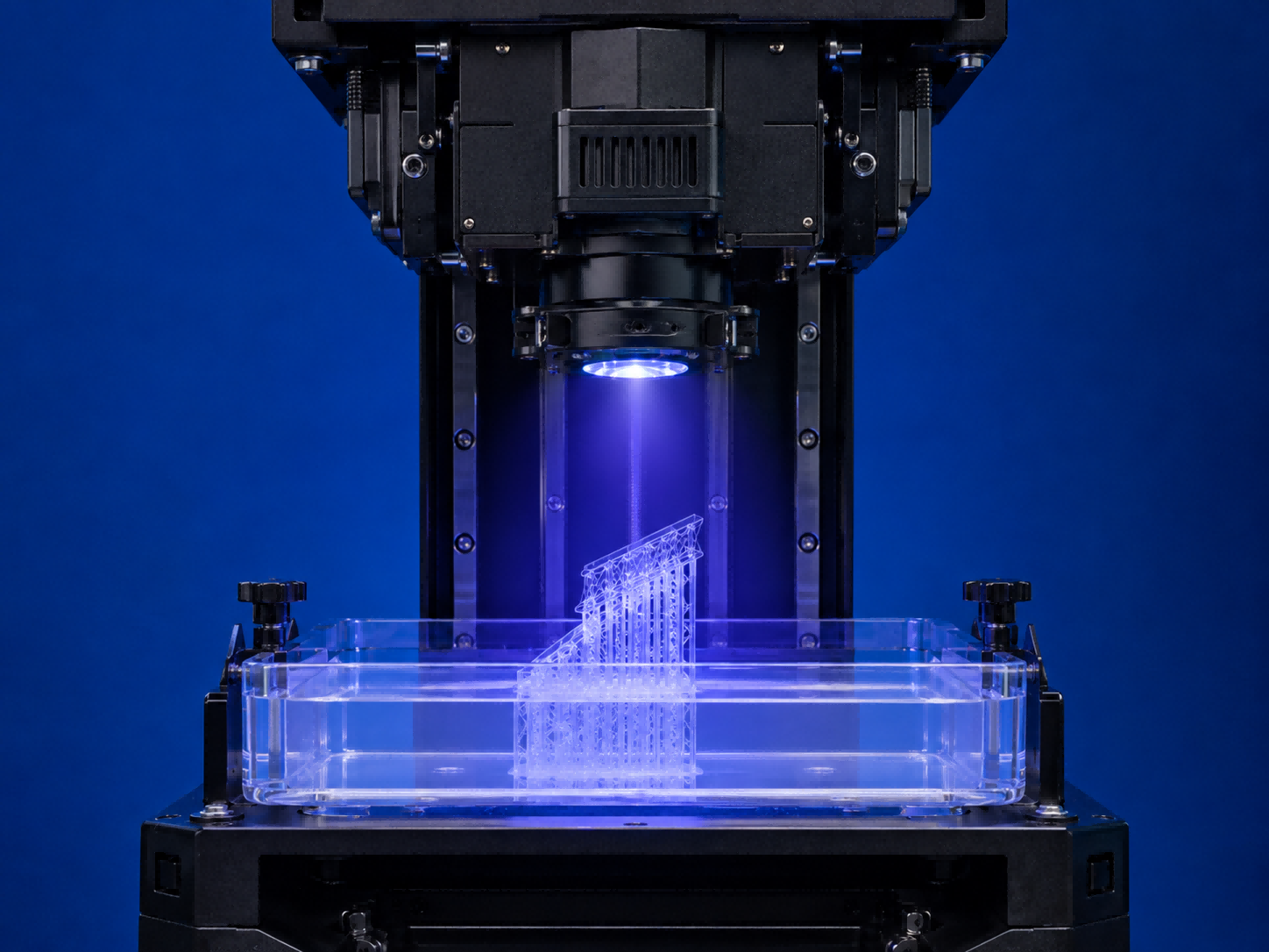
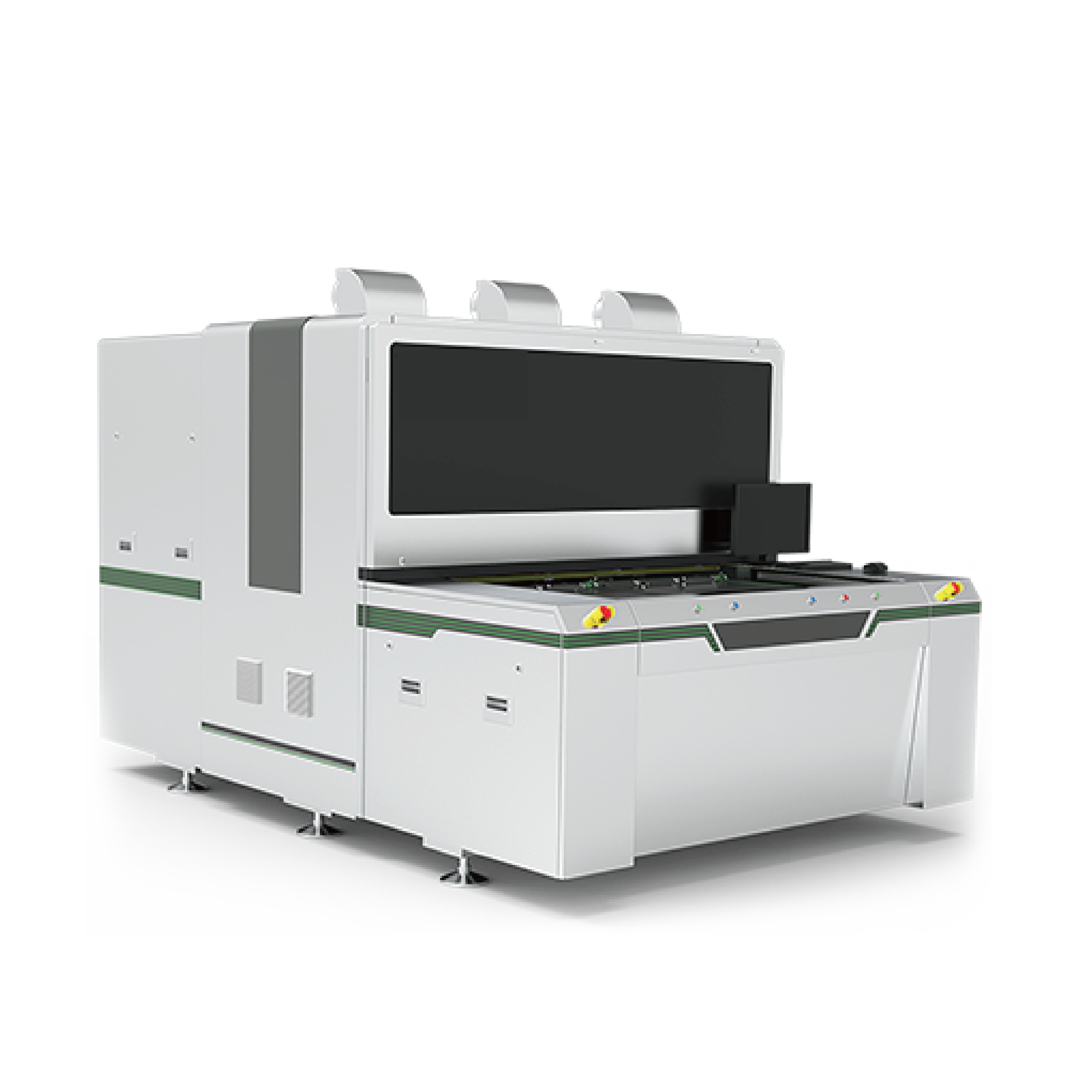
LDI (Laser Direct Imaging) is a new‑generation mask‑free digital photolithography technology. Its fundamental principle: a computer directly parses CAD/Gerber digital files of PCBs, IC substrates and display panels, precisely controls ultraviolet laser beams, and projects patterns onto board‑surface photoresist or solder‑mask ink without physical film masks.Essentially digital photolithography, LDI realizes a fundamental shift from “analog mask‑based imaging” to “digital‑signal‑driven direct imaging”. It eliminates physical errors introduced by conventional masks and acts as an essential manufacturing process for high‑end PCBs, advanced packaging and precision display devices.Solder‑mask‑dedicated LDI is a specialized variant optimized for harsh operating conditions: thick pigment‑loaded solder‑mask inks, copper thickness steps on substrates, and variable photosensitivity across multi‑color inks. It addresses industry‑wide pain‑points in conventional solder‑mask processing such as uneven curing, insufficient accuracy and low yield, and has become a standard upgrade for high‑end PCB solder‑mask workflows.
2. Solder‑Mask LDI Process Principle and Overall Equipment Architecture
2.1 Standard Full Solder‑Mask Process Flow
LDI laser exposure is a critical step embedded within the complete manufacturing chain. The standard sequence is shown below:Surface pre‑treatment (degreasing, board grinding, dust removal) → Solder‑mask coating (electrostatic spraying / curtain coating) → Pre‑bake (tack‑free drying to evaporate ink solvent) → Precision LDI laser exposure → Development (unexposed ink washed away by weak‑alkaline solution) → Post‑cure (high‑temperature full hardening) → Visual inspection and performance verification
2.2 Core Imaging Principle of Solder‑Mask LDI
2.2.1 Photochemical Response of Inks
Negative‑working LPI solder‑mask inks dominate industrial practice. Upon laser irradiation, ink resin undergoes cross‑linking and curing to form a developer‑resistant stable layer permanently bonded to the substrate for insulation protection. Non‑irradiated regions remain chemically unchanged and are fully removed by weak‑alkaline developer to expose copper at pads and gold fingers.
2.2.2 Imaging Logic for Digital Files
Solder‑mask Gerber files follow negative‑polarity logic and can be parsed directly without manual conversion. Black masked zones in files correspond to circuit‑protection areas and receive laser exposure for curing. White transparent zones define opening areas where the laser is turned off, and patterns are formed in subsequent development. Manual conversion‑induced errors are entirely avoided.
2.3 Core Architecture of Solder‑Mask‑Dedicated LDI Equipment
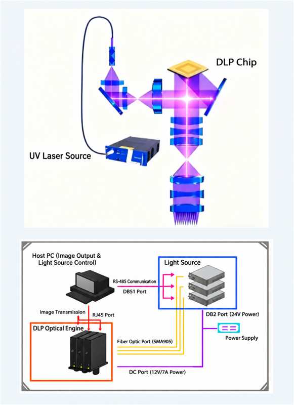
Distinct from conventional dry‑film LDI for circuit traces, solder‑mask‑specific LDI equipment features specialized optical optimization targeting thick pigment‑bearing inks, multi‑color formulations, copper thickness steps and curing uniformity. It consists of two primary assemblies — the UV laser source system and precision DMD optical engine — together with auxiliary modules for alignment, focusing and motion control.
2.3.1 UV Laser Source (Energy Core)
Delivers stable ultraviolet energy for ink photochemical reactions and matches photosensitivity requirements of multi‑color solder‑mask inks. 405 nm UV semiconductor lasers are widely adopted for strong penetration, stable power and compatibility with thick‑film inks. They efficiently penetrate pigment‑loaded green, black and white inks and mitigate under‑exposure and pseudo‑dry ink peeling. Shorter‑wavelength 355 nm sources offer superior resolution yet limited penetration, and are mostly deployed for fine‑line processing rather than solder‑mask applications. Premium systems adopt multi‑band light sources covering 365 nm, 385 nm and 435 nm to support the full spectrum of solder‑mask inks.
2.3.2 DMD Precision Optical Engine (Imaging Core)
As the heart of digital imaging, it performs beam shaping, pattern modulation and precision projection. Key sub‑modules and functions are listed below:
Beam Shaping & Homogenizing Module: Converts Gaussian beams into uniform top‑hat profiles, eliminates intra‑panel energy deviation, prevents local over‑exposure / under‑exposure, guarantees whole‑board imaging consistency and enables seamless stitching between multiple optical‑engine fields‑of‑view.
DMD Digital Micromirror Device Array: Functions as a digital “electronic photomask”. Receives Gerber data commands and drives millions of micromirrors for independent tilting to modulate laser light paths and reproduce patterns error‑free.
Telecentric Projection Lens Group: Ensures near‑normal laser incidence onto substrates, compensates pattern distortion caused by copper thickness steps and board warpage, and improves flatness and accuracy of fine solder‑bridges and miniature openings.
Vision Alignment & Auto‑Focus Module: Micron‑level automatic fiducial recognition for alignment, dynamic compensation for board deformation and offset, paired with real‑time focusing to resolve defocus‑induced blurring.
3. Mainstream LDI Technical Routes and Core Imaging Advantages
Commercial LDI equipment falls into two categories: galvanometer scanning and DMD digital projection, suited for different accuracy and throughput requirements. The DMD tilt‑scan architecture represents the mainstream for high‑end solder‑mask and advanced‑packaging manufacturing.
3.1 Comparison of Two Technical Routes
3.1.1 Galvanometer Laser‑Scanning Route
High‑collimation laser beams are steered by high‑speed galvanometers or rotating prisms with F‑theta lenses for large‑format scanning exposure. Strengths include high beam quality, stable imaging, large field‑of‑view and balanced throughput for mass production of large standard panels; fine‑feature imaging capability is limited.
3.1.2 DMD Digital‑Projection Scanning Route
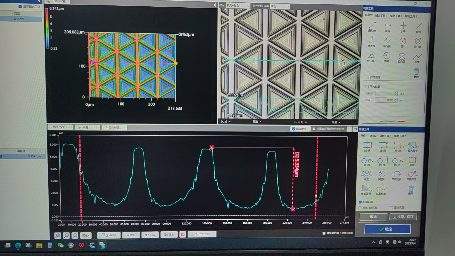
Laser light passes through fiber coupling and beam homogenization before illuminating the DMD chip. Pattern‑modulated light is projected onto substrates via projection lenses with multi‑field stitching, delivering high imaging flexibility and superior achievable resolution. Two generations exist: conventional step‑and‑repeat “stamp‑style” exposure suffers low throughput, severe stitching‑induced Mura artifacts and poor uniformity and is gradually phased out. DMD tilt‑scan technology is today’s high‑end mainstream solution.
3.2 Core Advantages of DMD Tilt‑Scan Technology
The DMD chip is mounted at a predefined tilt angle (1.79°, 3.57°, 7.12°, 14.03°), misaligning the pixel grid relative to the scanning direction and enabling multi‑pixel offset sampling and superposition during exposure. Equivalent resolution is boosted by 1.2‑1.5×. Pixel jagged edges, stitching artifacts and pattern distortion are substantially eliminated. Overlay accuracy and pattern‑edge smoothness are greatly enhanced, perfectly satisfying requirements for ultra‑fine solder‑bridges and miniature openings.
4. Comprehensive Comparison: Solder‑Mask LDI versus Conventional Film‑Based Exposure
Advantages of LDI over legacy workflows are analysed across four dimensions: accuracy & quality, production flexibility, manufacturing cost and process compatibility.
4.1 Accuracy and Quality
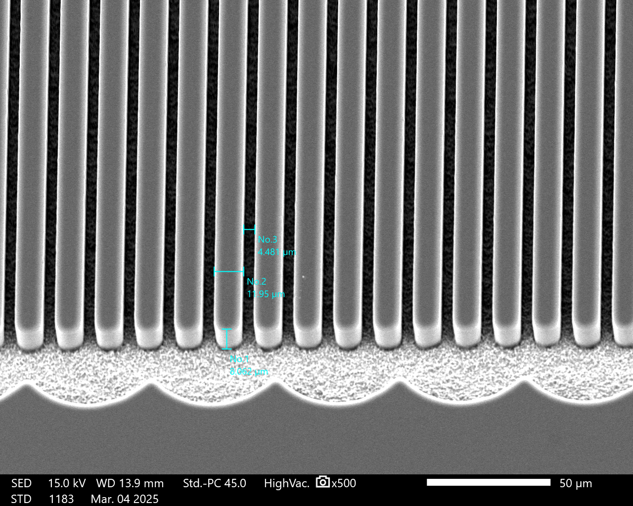
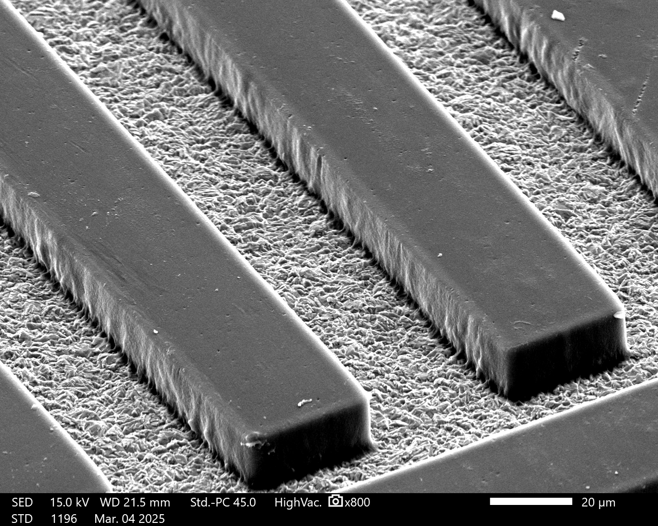
Conventional film exposure suffers from thermal expansion / contraction, film wear and contamination, plus manual alignment errors. Opening offsets are significant, requiring ≥50 μm single‑sided opening allowance. Ultra‑fine solder‑bridges are prone to fracture and deformation; resist bridging and solder‑bridging defects occur frequently.Free of physical film media, solder‑mask LDI achieves digital alignment accuracy within ±15 μm and supports 1:1 zero‑allowance precise openings. Solder‑bridges as fine as 20 μm can be reliably formed with smooth, jag‑free pattern edges. Structurally‑related defect rates drop dramatically.
4.2 Production Flexibility and Lead Time
Traditional processing requires dedicated film fabrication, storage and replacement for each part number. Product change‑overs are cumbersome and time‑consuming, ill‑suited for high‑mix low‑volume fast‑turnaround demands.LDI requires no consumables. Product switching only loads different digital files; model change‑over completes within seconds. Lead times for prototyping and mass production are shortened, matching trends toward custom PCB manufacturing.
4.3 Production Cost
Film‑based processing incurs recurring expenses for film production, replacement and maintenance. Rework and scrap caused by manual mis‑alignment and film contamination keep overall long‑term costs high.LDI involves mainly one‑time capital equipment expenditure with no recurring consumable costs. Labour requirements are reduced, while stable batch yield and low rework rates yield lower long‑term total cost‑of‑ownership.
4.4 Process Compatibility Boundaries
Conventional film exposure is largely limited to basic low‑density PCBs and entry‑level single‑/double‑layer consumer‑electronics boards and cannot meet high‑precision requirements. LDI supports the full spectrum of high‑end products including general‑purpose boards, HDI, automotive‑grade boards, high‑frequency high‑speed boards, IC substrates, Mini‑LED panels and heavy‑copper power PCBs.
5. Nine Core Key‑Technologies and Process Challenges for High‑End LDI
High‑performance solder‑mask LDI represents a sophisticated interdisciplinary technology integrating laser optics, precision mechanics, high‑speed algorithms, intelligent control and thermal stabilization. Nine core technical challenges define equipment accuracy and stability barriers.
5.1 Multi‑Band High‑Stability Laser‑Source Technology
To accommodate variable photosensitivity of multi‑color solder‑mask inks, mixed‑wavelength sources covering 365 nm / 375 nm / 385 nm / 405 nm / 435 nm are required, supporting both circuit‑trace exposure and solder‑mask curing. Lasers must deliver stable power, long service life and low etendue, while solving fibre‑end damage and beam degradation under high power to ensure long‑term batch‑to‑batch energy consistency.
5.2 High‑Uniformity Precision Optical‑Engine Technology
Incorporates high‑performance beam‑homogenizing modules, high‑MTF low‑distortion projection lenses and low‑stray‑light optical architectures. Optical distortion and thermal drift are tightly controlled to avoid local over‑/under‑exposure across panels, ensuring faithful pattern reproduction and even energy distribution.
5.3 High‑Precision Dynamic Auto‑Focus Technology
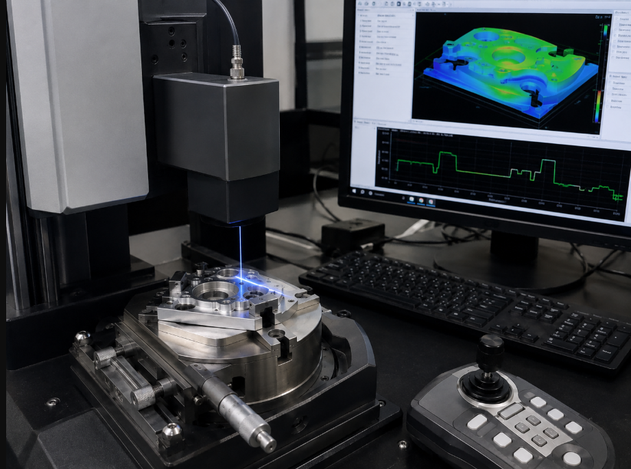
High‑end lenses feature shallow depth‑of‑field. Board warpage and copper thickness steps readily produce defocus blur. High‑precision line‑laser profilers acquire 3D point‑cloud data of board surfaces. Paired with dual‑wedge lens focusing modules, dynamic focus adjustment of 0.3 μm resolution over 30 μm travel keeps substrates consistently within effective depth‑of‑field during exposure.
5.4 Full‑Dimensional Intelligent Algorithm Compensation Technology
Integrates core algorithms: raster pattern generation, tilt mapping, grayscale modulation, dose compensation, stitching compensation and distortion correction. Board deformation, optical path deviation and stitching errors are comprehensively corrected for real‑world mass‑production operating conditions.
5.5 Ultra‑High‑Speed DMD Image Refresh Technology
Supports scan frequencies of tens of kHz. Multi‑GB high‑resolution image datasets are processed and transmitted in real‑time for fast, accurate micromirror actuation, eliminating pattern smearing and distortion during high‑speed scanning.
5.6 Microsecond‑Scale Multi‑Module Synchronization‑Control Technology
Enables microsecond‑level synchronized coordination of stage motion, laser triggering, DMD image refresh and focus adjustment. Timing‑mismatch‑induced pattern shift and distortion are prevented to preserve accuracy under high‑throughput operation.
5.7 Global Thermal‑Stability Control Technology
Heat generated by lasers, DMD chips and drive electronics during continuous operation causes thermal drift, lens deformation and optical‑parameter shift. Global temperature control and optimized thermal management suppress thermal errors for sustained high‑precision equipment performance.
5.8 Intelligent Exposure‑Dose Equalization Technology
Tilt‑scan mode requires multi‑pass pixel superposition within local zones. The system dynamically adjusts exposure dose according to scan passes and pixel‑superposition counts, achieving highly uniform delivered dose across the entire exposure field.
5.9 Ultra‑Precision Motion‑Control Technology
High‑speed stages with excellent repeat‑positioning accuracy precisely synchronize with optical imaging cycles, balancing mass‑production throughput and micron‑level positioning precision.
6. In‑House‑Developed Core Product Solutions and Field‑Proven Advantages
Targeting industry‑wide pain‑points for solder‑mask exposure, fine‑line processing and advanced packaging, fully in‑house‑developed LDI hardware‑and‑software stacks deliver end‑to‑end controllability for high‑end mass‑production requirements.
6.1 Multi‑Band High‑Stability Laser‑Source Solution
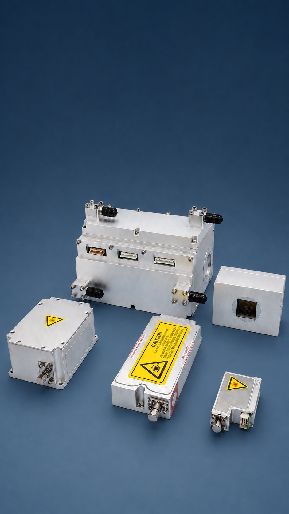
Self‑developed full‑spectrum UV laser sources (375 nm / 405 nm / 425 nm / 435 nm) deliver maximum output power of 150 W, covering circuit‑trace exposure, full‑color solder‑mask exposure and semiconductor advanced‑packaging exposure scenarios. Optimized laser collimation and fibre‑coupling precision mitigate fibre‑end damage and beam attenuation under high power. Both water‑cooled and air‑cooled variants are offered balancing long lifetime and stability.
6.2 TTL High‑Frequency Modulated Laser‑Source Solution
Abandons conventional continuous‑wave (CW) operation and adopts TTL high‑frequency pulse modulation precisely synchronized with DMD micromirror timing. Supports pulse‑modulation frequencies up to 100 kHz. At 20 kHz / 50 % duty‑cycle, response latency reaches 324 ns with rise‑ / fall‑times of merely 28 ns. Scanning smearing and soft‑edging artifacts are eliminated, improving pattern‑edge contrast and imaging fidelity significantly.
6.3 Hybrid LED+LD Illumination‑System Solution
Addresses uneven solder‑mask colouring and poor ink compatibility stemming from single‑wavelength laser sources. Combines 365 nm / 385 nm UV‑LEDs and 405 nm / 435 nm laser sources. Each LED channel outputs 14 W; each laser channel peaks at 150 W. It replicates broad‑spectrum benefits of traditional mercury lamps while retaining laser‑grade stability and high power, fully compatible with green, black and white solder‑mask inks.
6.4 9900 Integrated DLP Optical‑Engine System
Built upon “in‑house core‑module development plus system‑level integration”. Tightly synergizes light sources, microlens‑arrays, high‑precision lenses and auto‑focus assemblies. Standardized interfaces and unified control platforms resolve known limitations of conventional optical engines: poor inter‑module coordination, parameter mismatch and large thermal drift. Sealed mechanically‑stable construction offers good environmental robustness and supports modular customization for high‑precision exposure across solder‑mask, fine‑line and advanced‑packaging use‑cases.
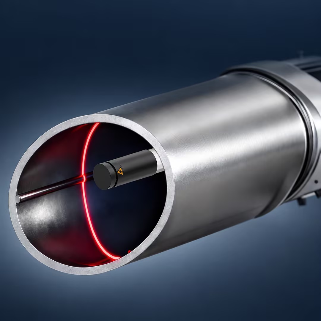
6.5 Line‑Laser Profiler plus AF Auto‑Focus System
A high‑precision line‑laser profiler with 200 nm Z‑axis repeat‑measurement accuracy rapidly reconstructs 3D surface point‑cloud models and calculates depth‑of‑field parameters across the board. Combined with proprietary AF focusing algorithms and dual‑wedge lens modules, dynamic focus tuning with 0.3 μm resolution over 30 μm travel eliminates defocus blurring and soft‑edge defects caused by board warpage and thickness variation.
6.6 MLA Microlens‑Array High‑Precision Exposure Solution
Microlens‑array optics finely compress and shape individual DMD pixel beams. Combined with mature DMD tilt‑scan processing, imaging resolution and exposed area are enhanced without throughput sacrifice. Stitching uniformity is improved to achieve simultaneous high accuracy and high throughput for ultra‑fine solder‑mask and fine‑line manufacturing.
7. Real‑World Deployment and Core Value across Segmented Application Scenarios
LDI technology resolves process‑specific bottlenecks in diverse high‑end PCB fields and satisfies stringent mass‑production specifications. Key deployment cases are summarised below.
7.1 Consumer‑Electronics HDI / Any‑Layer Interconnect PCBs
Core Pain‑Points: High‑density routing; fine‑pitch BGA pads prone to solder‑mask mis‑registration, solder‑bridge fracture and solder‑bridging short‑circuits. Fast‑changing product portfolios and long film‑based change‑over cycles impede fast low‑volume prototyping.Solution: Mask‑free digital imaging plus dynamic deformation compensation delivers micron‑accurate openings and stable ultra‑fine solder‑bridge formation. Part‑number switching completes within seconds via digital‑file loading.Value: Structurally‑related solder‑mask defect rates reduced by >80 %; prototyping lead‑time shortened by 60 %. Empowers manufacturers to secure orders for high‑precision consumer‑electronics PCBs.
7.2 Automotive‑Grade PCBs
Core Pain‑Points: Harsh on‑vehicle operating environments. Conventional contact film exposure risks surface scratching and particle contamination. Uneven curing causes solder‑mask delamination and insulation failure, failing automotive‑grade reliability requirements.Solution: Non‑contact laser exposure with highly uniform energy output eliminates surface damage and contamination. Solder‑mask layers achieve uniform curing and excellent adhesion performance.Value: Meets AEC‑Q100 automotive‑grade qualification criteria. Prevents large‑scale reliability‑related field failures and lowers warranty‑claim costs. Enables access to core supply‑chains for new‑energy vehicles and autonomous driving.
7.3 5G Communication / Server High‑Frequency High‑Speed PCBs
Core Pain‑Points: High‑frequency substrates impose strict requirements for impedance control and signal integrity. Film‑induced dimensional shift causes impedance drift, signal interference and transmission anomalies.Solution: Fully digital imaging free from physical deformation yields highly consistent feature dimensions and clean edges free of residual ink. Uniform insulation spacing stabilizes impedance performance.Value: Greatly improves electrical‑performance consistency of high‑frequency boards and reduces scrap rates for premium substrates. Supports mass‑production for 5G base‑stations and high‑end servers.
7.4 Mini‑LED / Micro‑LED Display Substrates
Core Pain‑Points: Highly‑reflective white inks often suffer surface‑only curing and subsurface pseudo‑dry conditions. Residual developer‑insoluble ink and ink peeling are frequent. Uneven openings over tiny pads cause luminance non‑uniformity and pixel defects.Solution: Special long‑wavelength high‑penetration light sources paired with intelligent dose adjustment realize synchronized through‑thickness curing for light‑coloured inks and precise micro‑zone light control.Value: Resolves chronic curing‑related issues for white solder‑mask inks and drastically lowers display‑panel defect rates. Complies with mass‑production standards for ultra‑high‑density LED substrates.
7.5 IC Substrates and Advanced‑Packaging Substrates
Core Pain‑Points: Ultra‑fine pin pitches. Conventional‑process accuracy is insufficient; resist bridging and solder‑bridge fracture lead to chip‑packaging short‑circuits and device failure.Solution: High‑precision DMD‑controlled imaging with tilt‑scan reliably forms ultra‑fine packaging‑grade features, delivering superior alignment accuracy and consistency.Value: Satisfies ultra‑high‑precision manufacturing thresholds for semiconductor packaging and improves packaging yield, facilitating access to high‑end semiconductor supply‑chains.
7.6 New‑Energy Industrial‑Control Heavy‑Copper Power PCBs
Core Pain‑Points: Severe copper‑thickness steps and variable ink film thickness across substrates. Conventional exposure yields uneven energy distribution: over‑exposure in thin regions and insufficient curing in thick regions. Solder‑mask delamination and high‑temperature insulation failure occur.Solution: High‑performance beam‑homogenizing system plus zone‑wise fine energy tuning adapts to thick‑film‑ink exposure requirements and delivers sufficient through‑thickness curing.Value: Resolves uneven curing challenges for heavy‑copper PCBs. Enhances thermal‑resistance, solder‑resistance and insulation reliability for long‑term stable operation of new‑energy industrial‑control equipment.
8. Solder‑Mask LDI Process‑Control Key‑Points and Manufacturing Challenges
8.1 Unique Core Challenges for Solder‑Mask LDI
Solder‑mask LDI is significantly more demanding than conventional dry‑film LDI for circuit traces. Three major challenges prevail: first, vastly different light‑absorption characteristics among green, black and white pigmented inks place stringent requirements on source wavelength and exposure‑dose matching; second, copper‑thickness‑step‑driven ink‑thickness variation complicates uniform laser penetration depth; third, pre‑baked inks exist in semi‑solid state with narrow process windows, readily leading to over‑exposure or under‑exposure defects.
8.2 Key Mass‑Production Control Guidelines
Light‑Source Energy Management: Dynamically match exposure dose to ink colour and film thickness. Increase delivered energy specifically for black and white inks to guarantee full subsurface curing.
Optical‑System Management: Periodically calibrate beam‑homogenizing modules and projection lenses to ensure panel‑wide energy uniformity and absence of optical‑path drift.
Deformation‑Compensated Alignment Control: Enable dynamic deformation compensation to automatically correct board warpage and stretch‑induced offset and guarantee accurate opening registration.
Pre‑Processing of Input Data: Optimize Gerber datasets accounting for LDI imaging behaviour; fine‑tune dimensions for fine solder‑bridges and openings to fit practical process windows.
9. Future Technology Trends and Equipment‑Selection Recommendations
9.1 Future LDI Evolution Directions
Ultra‑High‑Precision Advancement: Wider adoption of 355 nm / DUV short‑wavelength sources for improved optical resolution enabling mass‑production of 1‑5 μm ultra‑fine features for advanced‑packaging workflows.
Intelligent Upgrading: Integration of AI‑driven real‑time vision compensation and adaptive intelligent dose tuning to boost overlay accuracy and production yield.
Smart‑Factory Integration: Adoption of digital‑twin technology for on‑board self‑inspection, autonomous parameter calibration and predictive maintenance for unmanned smart‑factory environments.
Cross‑Domain Process Expansion: Deeper adaptation to glass substrates, Chiplet packaging, RDL processes and Micro‑LED manufacturing to broaden application boundaries.
LDI Laser Direct Imaging, empowered by mask‑free digital imaging advantages, has revolutionized legacy analog film‑based lithography. It fundamentally addresses well‑known industry‑wide limitations of conventional workflows: low accuracy, poor consistency, limited flexibility, high consumable costs and elevated defect rates. Enabled by multi‑band laser sources, DMD tilt‑scan imaging, dynamic auto‑focusing and full‑dimensional algorithm compensation, LDI meets high‑volume high‑end solder‑mask‑manufacturing requirements across consumer electronics, automotive electronics, 5G communications, semiconductor packaging, new‑energy industrial‑control and precision‑display sectors.As downstream end‑products continue advancing toward higher precision and performance, alongside rapid development of AI computing power, advanced packaging and smart‑manufacturing infrastructure, LDI will keep evolving and gradually establish itself as the standard core manufacturing process for PCB solder‑mask production, fine‑line processing and advanced‑packaging lithography. Fully in‑house‑developed LDI hardware‑and‑software stacks achieve full‑link domestic controllability and deliver high‑accuracy, high‑stability, high‑flexibility and cost‑effective digital mass‑production solutions for PCB manufacturers. It supports process upgrading, cost reduction & efficiency improvement and market expansion into high‑end segments.