










Stable Operation for Over 10 000 Hours! This UV Laser Light Source Helps You Reduce Costs and Improve Efficiency
Product Details
Aug 20,2026
Driven by rapid development in precision manufacturing, biotechnology, semiconductors and other industries, processing tools are facing increasingly stringent requirements for accuracy, adaptability and stability. Whether it is fine‑line exposure for PCBs, precise micro‑nano lithography, or analysis of deep‑cell functions in biological detection, conventional laser light sources are often limited by single‑wavelength output, insufficient heat dissipation and short service life, and struggle to satisfy diversified production and R&D demands.Now, Litonics’ UV laser light source integrates multiple core advantages and delivers comprehensive performance breakthroughs to provide innovative solutions for industry‑wide challenges.In this edition of One‑Product Focus, we walk through the core strengths of Litonics UV laser light source and look ahead to a future empowered by advanced optical technology.
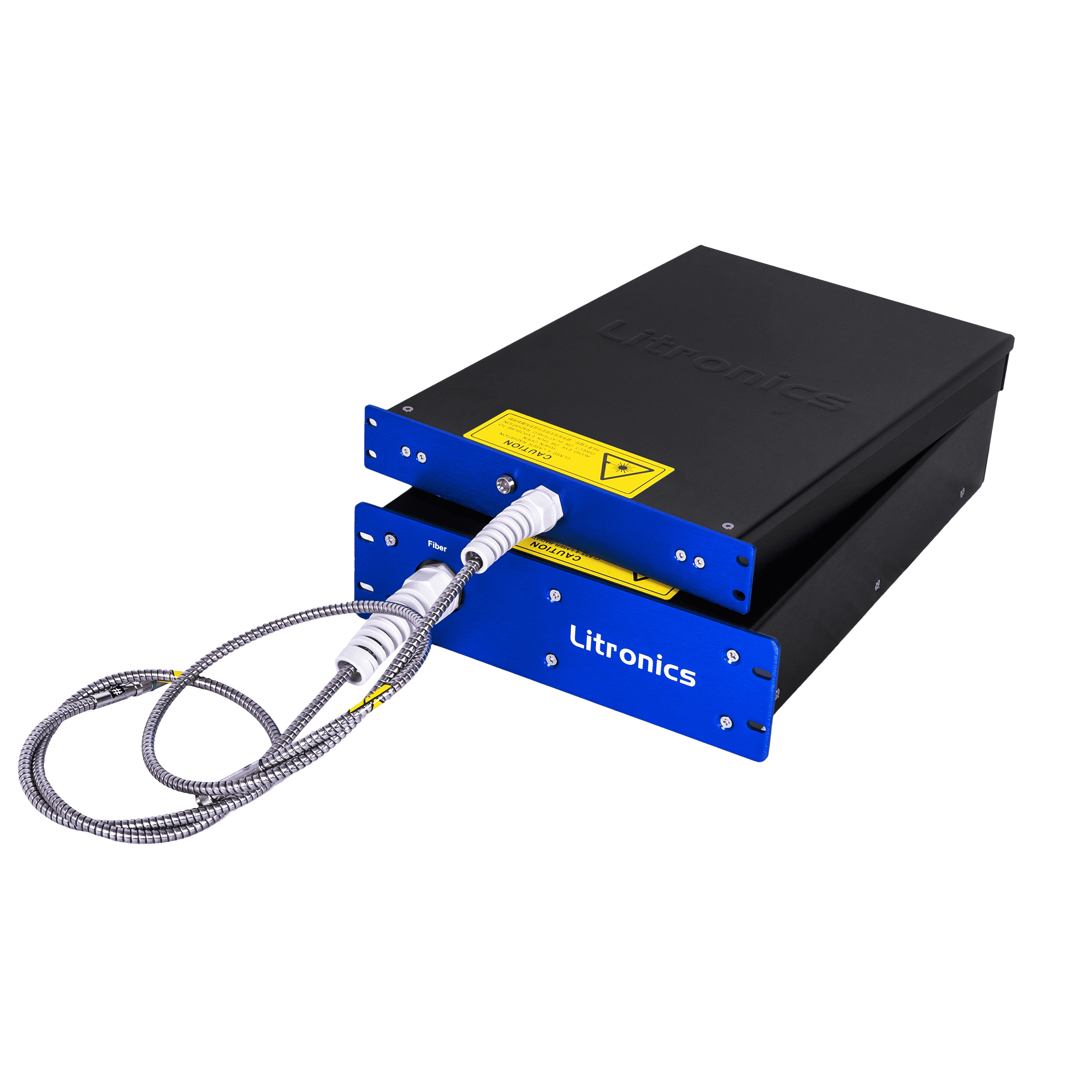
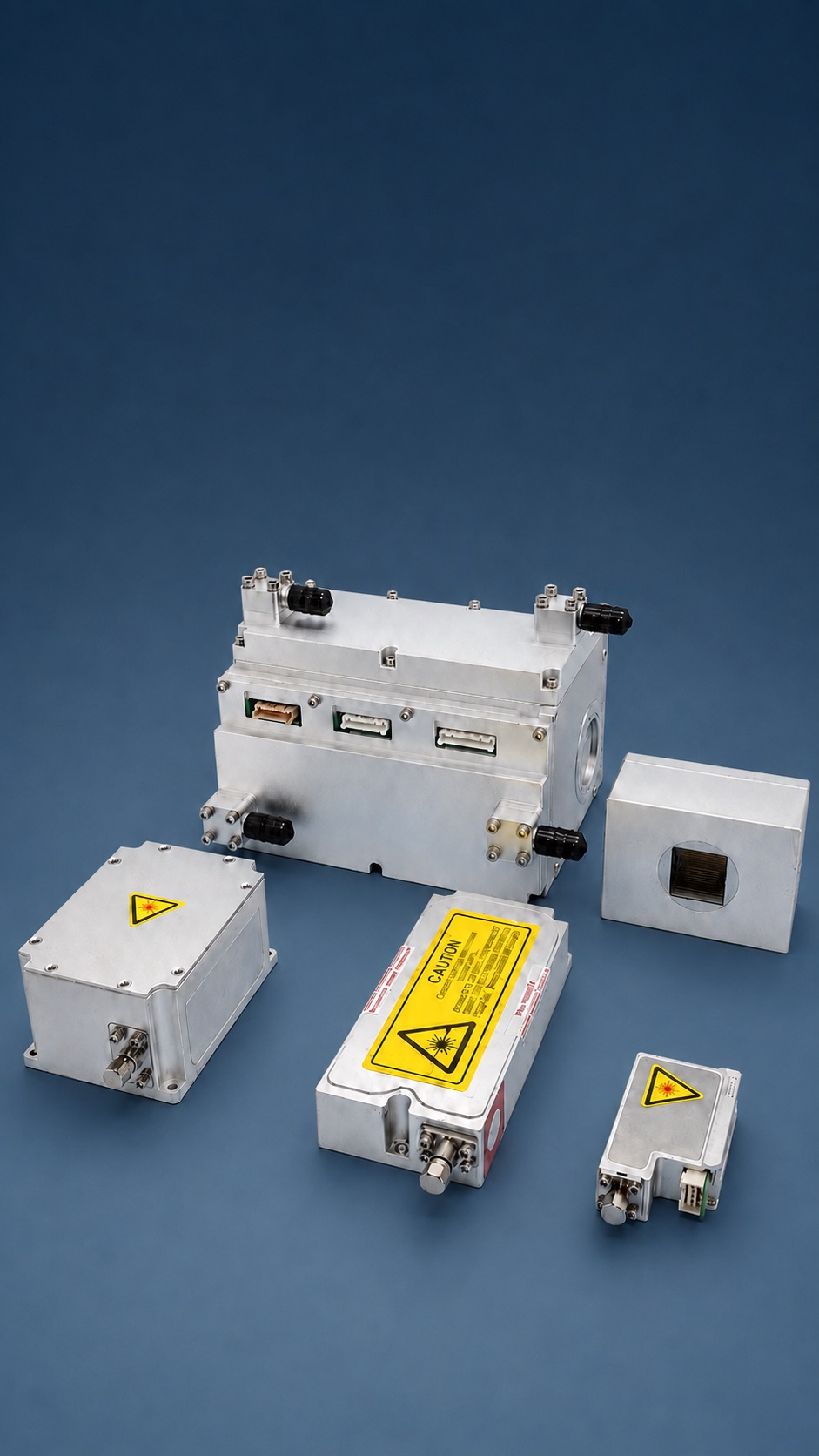
Water‑cooled
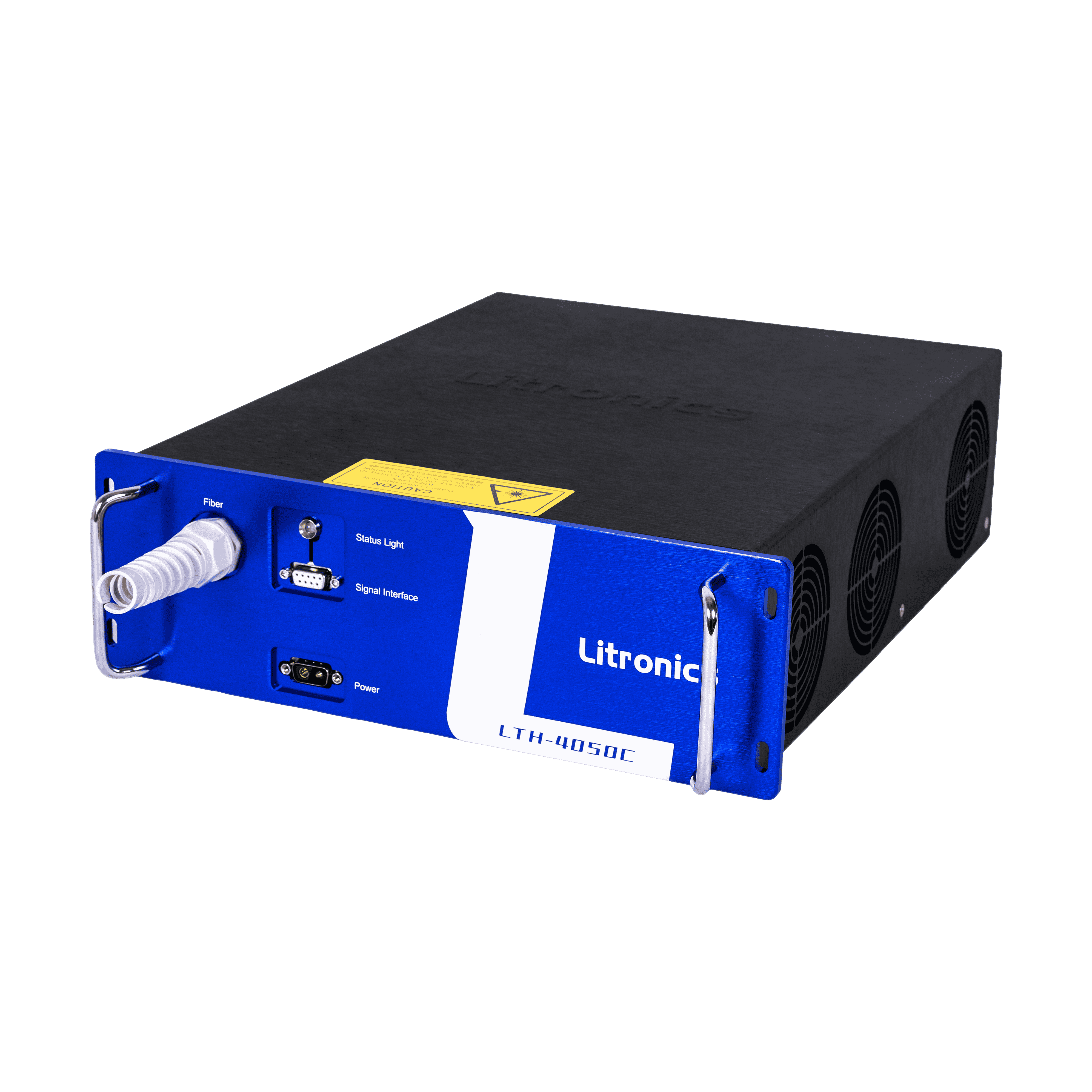
Air‑cooled
Product Features
Space‑coupling technology, peak wavelengths: 378 / 405 / 425 / 435 nmEquipped with multi‑peak‑wavelength design covering four key bands: 378 nm, 405 nm, 425 nm and 435 nm. Wavelength can be flexibly switched according to material properties and processing requirements. It supports diverse applications ranging from fine exposure of PCB circuits and inks to micro‑nano lithography and 3D printing.
Custom multi‑wavelength LEDs: replicate spectra of traditional light sources with boosted powerFurther mixed‑wavelength customization is available for LED sources such as 330 / 340 / 365 / 385 nm. Hybrid‑combining LEDs and lasers reproduces rich spectral characteristics of conventional light sources while elevating output power.
TEC air‑cooling or water‑cooling, compact structure for easy maintenanceThe light source adopts TEC‑based air‑cooling or water‑cooling thermal solutions tailored for different power‑level requirements, balancing compact mechanical layout and convenient servicing.
Long service life with high stability throughout operation lifetimeBoasting over 10 000‑hour service life and consistent performance over its lifespan, it fundamentally cuts overall operational costs and guarantees reliable operation for various application scenarios.
PWM (Pulse‑Width Modulation) or CW (Continuous‑Wave) output for flexible laser tuningOutput power: 4 W‑60 W @ TEC air‑cooling; 3 W‑150 W @ water‑cooling.
‑ PWM Mode: Precisely tune energy output by adjusting pulse frequency and duty cycle. Suitable for intermittent‑processing tasks such as DMD synchronization in laser direct imaging and fine‑feature curing for additive manufacturing. It mitigates material overheating and light diffusion induced by continuous irradiation.‑ CW Mode: Delivers stable continuous‑energy output for large‑area and high‑speed processing.
Speckle contrast < 4 % for improved beam quality
Laser speckle refers to uneven light‑and‑dark patterns originating from laser coherence. It degrades spot uniformity and consequently lowers processing accuracy and imaging clarity. Reduced speckle contrast means more even energy distribution across the laser spot with diminished light‑dark variation.
Product Applications
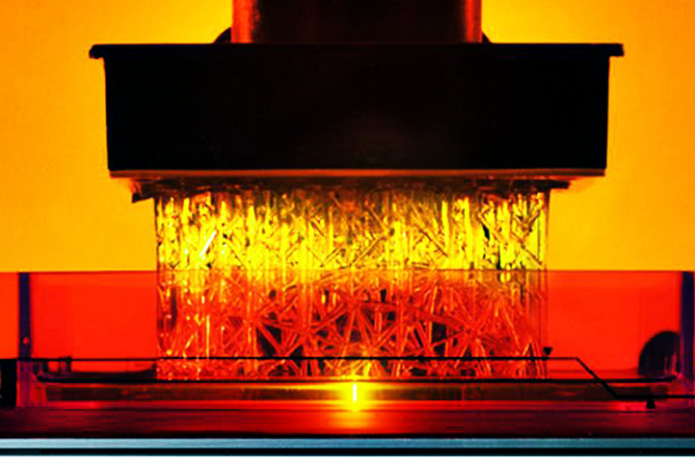
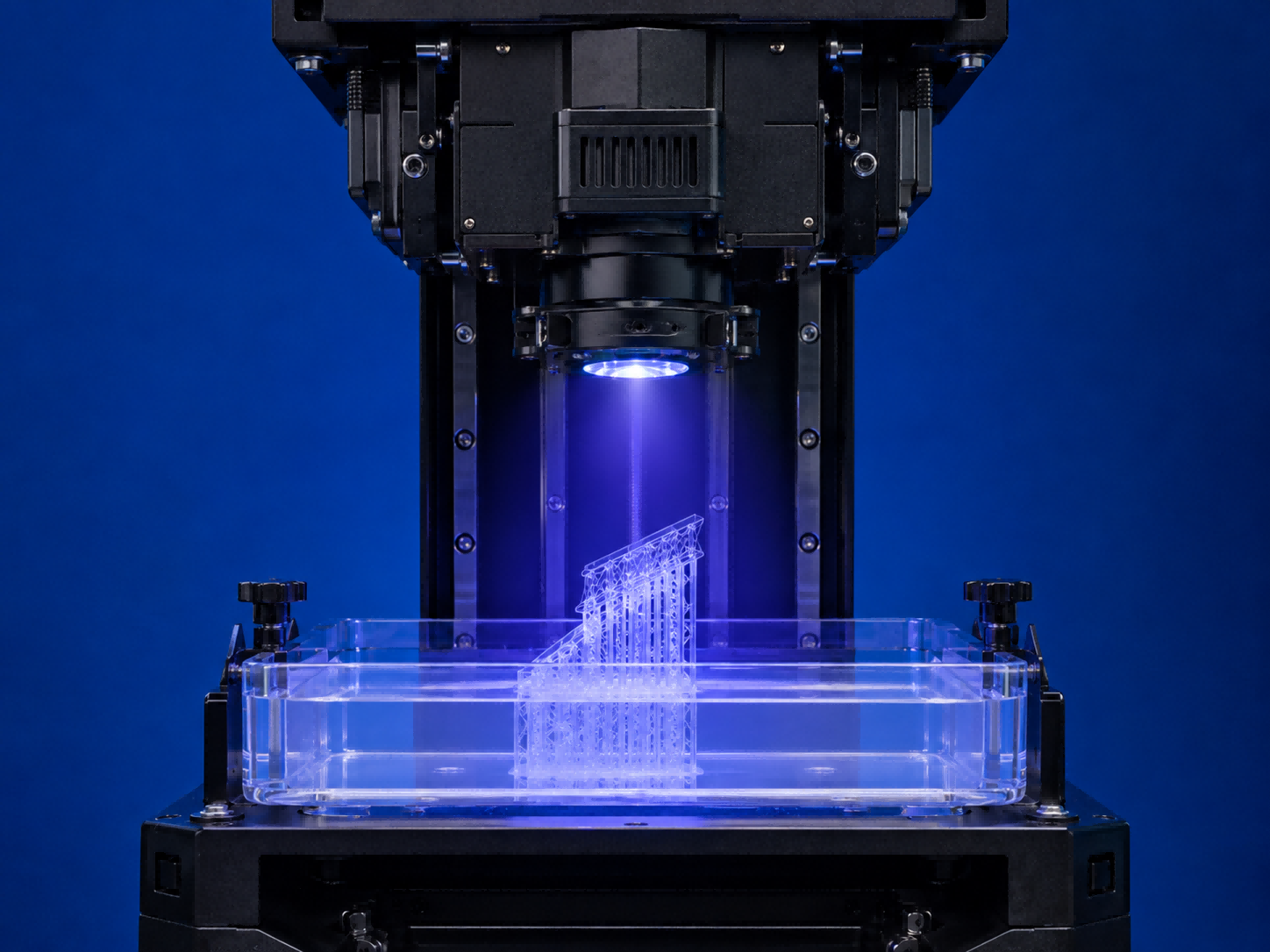
Additive ManufacturingThe UV laser cures resin via high‑efficiency area exposure using DLP‑chip imaging, which drastically accelerates printing speed. DLP technology enables fast and efficient fabrication of small‑size electronic‑component parts, toy accessories, microfluidic chips, footwear components and dental models.
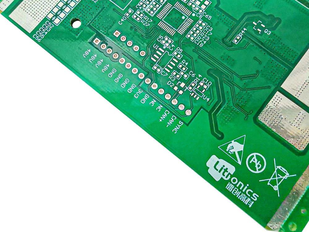
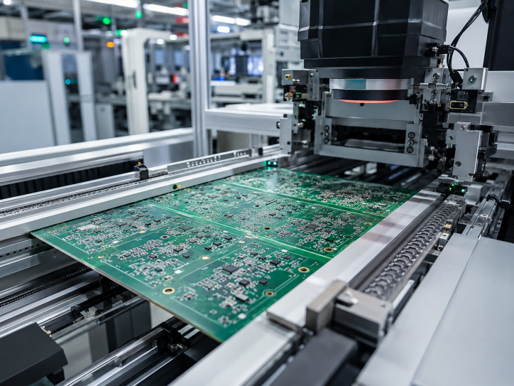
PCB ManufacturingLaser Direct Imaging (LDI) is a revolutionary technology for modern PCB manufacturing, especially for high‑density‑interconnect (HDI) boards, fine‑trace circuits and packaging substrates. It is gradually replacing traditional contact‑exposure methods. Typical uses include inner‑/outer‑layer circuit patterning, solder‑mask processing, and fabrication of high‑precision pads and markers. Featuring superior alignment and resolution accuracy, it improves yield, reduces defects, shortens production cycles, enhances process flexibility and enables higher circuit‑routing density.
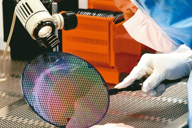
Advanced Semiconductor PackagingUV laser exhibits outstanding material compatibility. It precisely processes silicon, glass, ceramics and various polymer dielectric layers with micrometer‑scale accuracy and superior edge quality. This non‑contact processing effectively avoids thermal damage and mechanical stress introduced by conventional processes. It provides reliable process support for semiconductor devices toward higher integration density, finer pitch dimensions and heterogeneous integration, and acts as a core enabling tool driving continuous innovation in advanced‑packaging technologies.
As high‑end manufacturing advances rapidly, upgrades of core tools often propel progress across entire industries. This UV laser light source not only meets current processing demands but also adapts to future applications with higher precision and greater complexity, serving as a strategic equipment for enterprises pursuing long‑term growth.Taking light as the measuring rule and stability as the foundation. The UV laser light source ensures every beam of light illuminates a more precise world.