









From Component Inspection to Welding Tracking: How Line Laser Profile Sensors Safeguard Various Industries?
Product Details
Aug 20,2026
On Industry 4.0 production lines, every single micrometer can make or break outcomes. In the past, quality was assessed with calipers, white‑light devices and empirical judgment. Today, an ultra‑fine laser line sweeps across the target surface: within 0.1 seconds, profiles, defects and dimensions are captured in a single shot with micrometer‑level data accuracy. The line‑laser profile sensor acts like a 3D scalpel, uncovering invisible errors and delivering objective criteria for qualified products. Follow this laser line to rediscover what “precision” truly means.What unique strengths make it favored across numerous industries? Litonics introduces our Line‑Laser Profile Sensor in this product introduction.
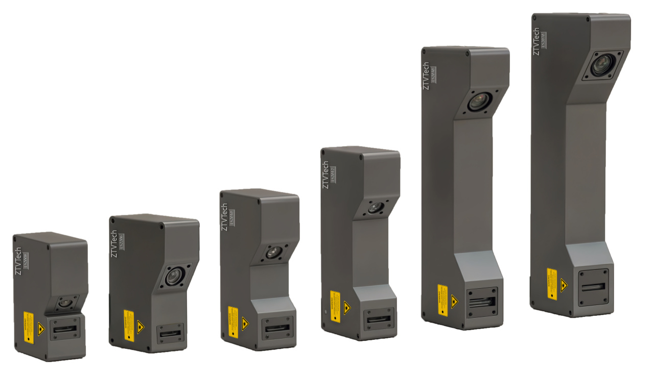
Line‑Laser Profile Sensor
Working Principle
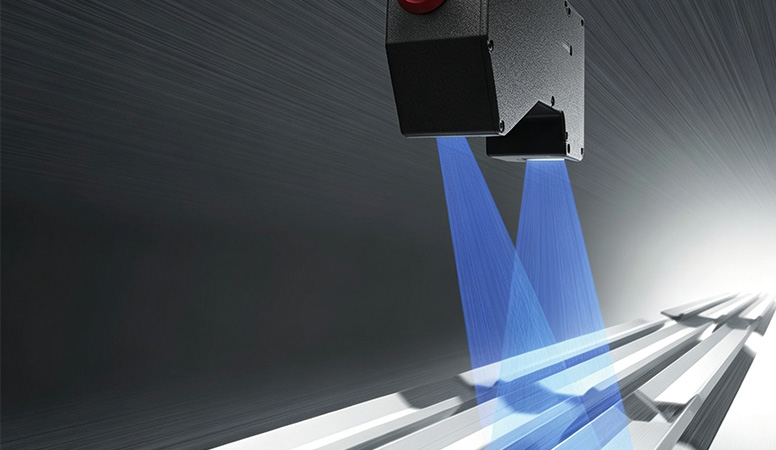
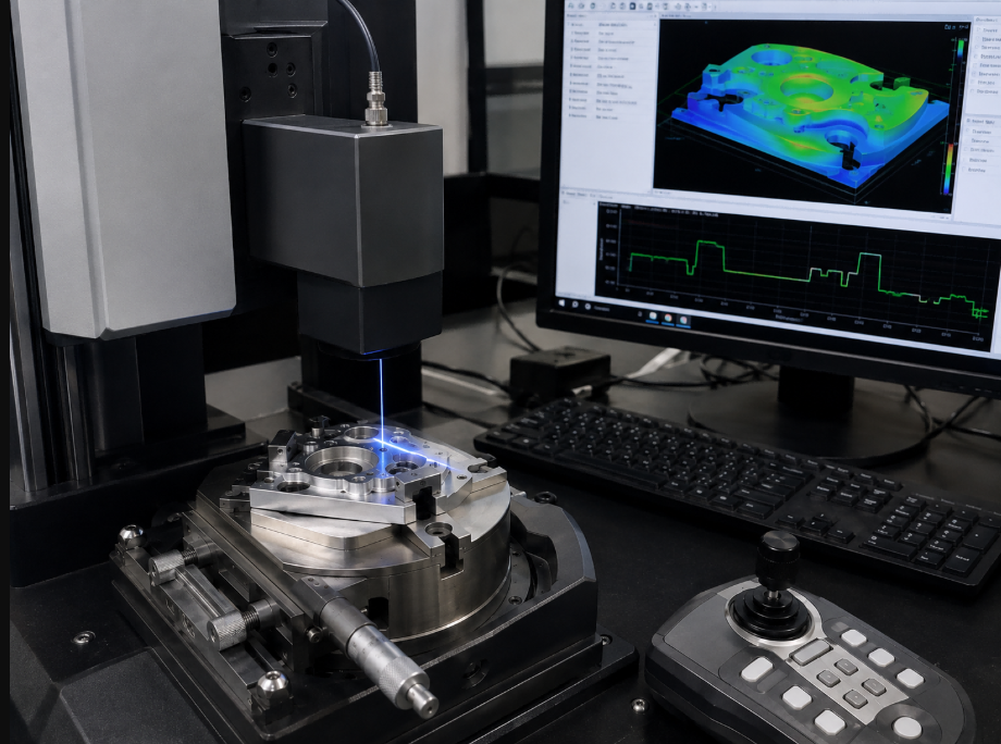
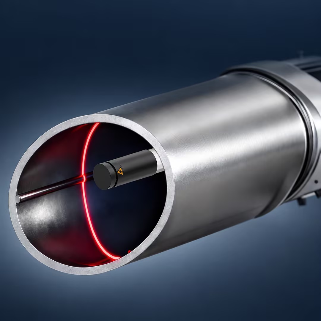
A line‑laser profile sensor is a 3D sensor based on the triangulation principle. An image sensor captures the laser‑line profile projected onto the object surface by a laser generator to reconstruct the object’s surface contour. One profile is acquired per exposure. The reflected laser line falls on different positions of the camera according to the distance between the target and the sensor. The laser emitter, camera and target form a triangle. See the schematic diagram below.
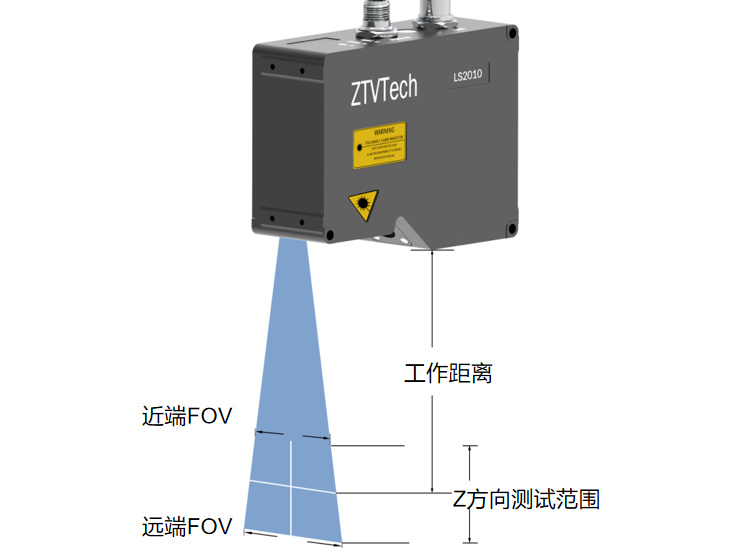
Schematic Diagram of Line‑Laser Profile Sensor Principle
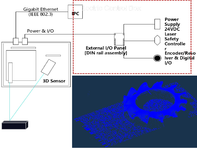
Core Technical Advantages
01 Micrometer‑level Z‑axis AccuracyUltra‑high physical resolution along the X‑axis for clear 3D object profile reconstruction;Z‑axis repeatability up to 0.2 μm.
02 High‑speed Scanning and Real‑time ProcessingFull‑profile data is obtained in one scan, far more efficient than point‑by‑point point‑laser scanning.FPGA‑accelerated algorithms enable microsecond‑level data processing with a maximum refresh rate of 8000 Hz.
03 Non‑contact Precision InspectionNo physical contact with measured objects (e.g. soft materials, precision electronic components), avoiding scratches or deformation.Adaptable to complex surfaces; capable of measuring high‑temperature, fragile or moving targets.
04 Robust Environmental AdaptabilityWide operating temperature range: ‑20 ℃ to +40 ℃ with built‑in temperature‑compensation algorithm.Operates under 10%‑95% RH non‑condensing humidity.IP67 dust‑proof and water‑proof rating with robust sealing performance.
05 Broad Software‑interface CompatibilityStandardized SDK interfaces, compliant with GigE Vision / GenICam protocols.Fully compatible with Windows / Linux operating systems.Supports multiple programming languages including C++ and C#.Seamlessly integrates with mainstream machine‑vision platforms such as LabVIEW and Halcon.
Typical Application Scenarios
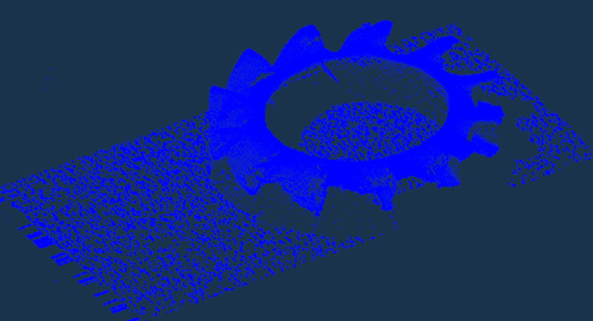
3D Inspection of Industrial Components
Full‑profile scanning with 0.2 μm repeat accuracy solves low‑efficiency manual sampling inspection and high missed‑defect rates for complex curved surfaces.
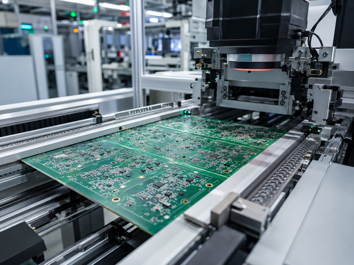
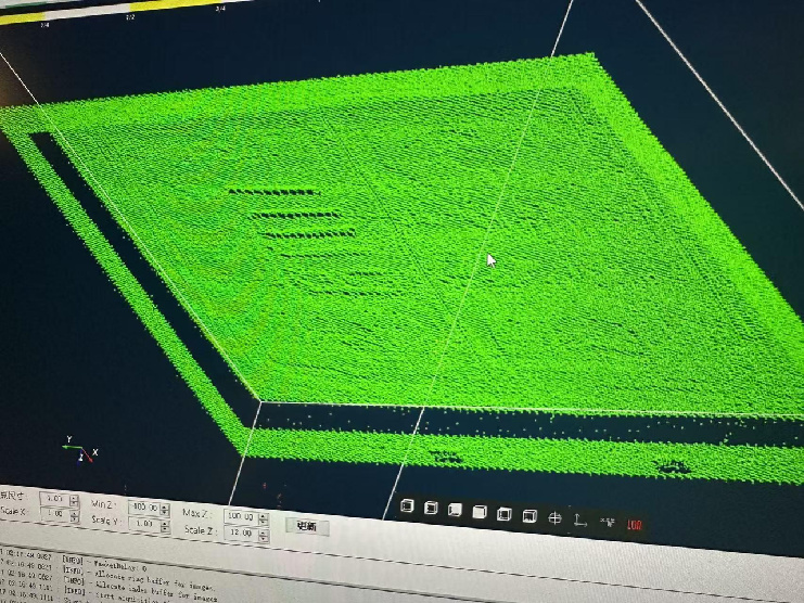
PCB Warpage Inspection
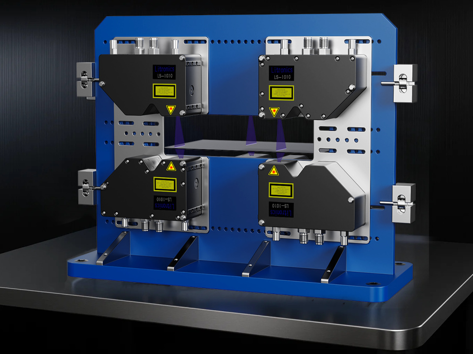
High‑precision 3D cameras perform automatic non‑contact online warpage measurement for circuit boards and effectively prevent print‑head collisions.
Wafer Sorting
Inspect thickness, line marks, TTV and warpage; achieve a sorting throughput of 20 000 wafers per hour.
Adhesive Bead Inspection
Real‑time measurement of adhesive bead height, width, volume and other parameters during dispensing processes. Automatic non‑contact detection for broken glue and glue overflow; adhesive weight estimation is also available.
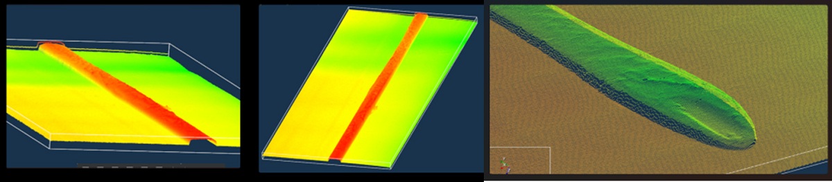
As modern manufacturing advances toward intelligence and higher precision, quality‑inspection standards for components keep rising. Against this backdrop, line‑laser profile sensors have become core instruments for critical workflows such as surface‑defect detection and dimensional measurement, thanks to non‑contact operation, micrometer‑level precision and high‑speed scanning, boasting broad application prospects.
We sincerely invite you to try our line‑laser profile sensor. Call us at 186‑0137‑1626 to apply for a free trial. Our technical team is ready to answer your inquiries at any time.